


Helen Xenos explains how the technology choices behind Ciena’s WaveLogic 6 Extreme 1.6 terabit coherent optics translate to optimal economic benefits for your network.
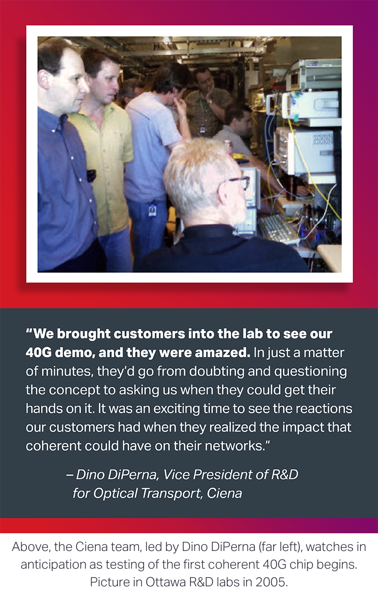 Coherent technology has revolutionized the way we communicate. Over the past 15 years, since we introduced the industry’s first coherent solution in 2008 (shown being tested by the team), Ciena’s WaveLogicTM innovations have enabled an incredible 20 times increase in data traffic over fiber and a more than 90% reduction in Watts/Gbps in our customers’ networks.
Ciena's long history of leadership in optical has been possible due to our engineers’ “never take no for an answer” attitude that has driven many impressive ground-breaking technology innovations over the last few decades, several of which changed the direction of the industry.
WaveLogic 6 is no different.
When you consider the next phase of your network evolution, you likely think, “Which technology aligns with where I want to go and will provide the best value for my investment?”. At Ciena when we design our next-generation coherent optics, we always keep that same question in mind. If you are going to make an upgrade, it needs to be worth it.
With our fifth technology generation, WaveLogic 5 Extreme (WL5e), we delivered the world’s first 800G to networks, and with >250 network deployments across all key geographical regions, WL5e has enabled ubiquitous 400G client connectivity, globally.
So, what choices did we make with WaveLogic 6 to push the industry forward?
The design objective was clear: provide significant improvements in cost and power efficiencies to justify onboarding new technology. But that’s not all. The natural next step was to deliver a whopping 1.6Tb/s and enough performance to support at least 800G per wavelength for any distance link in the network to support the next generation of routing data paths.
Let’s look at the technological innovations that will get us there.
Achieving the next generation
An effective way to increase data throughput over a single optical channel is to increase the baud, or symbol rate. The baud dictates the number of symbols transmitted per second, where each symbol consists of a number of bits as defined by the modulation scheme. More data is transmitted using fewer electronics and fewer electro-optical components, reducing cost, reducing energy consumption, and simplifying deployment.
To achieve double the capacity per wavelength versus 95Gbaud (800G technology) solutions, you need a modem with double the baud (~200Gbaud). That’s 200 billion symbols per second! As you can imagine, achieving this design is no easy feat. The first big hurdle is that a 200GBaud design requires high-bandwidth electro-optics as well as high-speed digital-to-analog and analog-to-digital-converters (DACs, ADCs) that have 100GHz of electrical bandwidth, which are simply not available. Additionally, there’s the challenge of fitting all this processing power into the same physical space as current solutions.
As the sixth generation of Ciena’s coherent offerings, WaveLogic 6 Extreme benefits from our team’s unmatched expertise in coherent networking and builds off of the technology and algorithms used in previous generations. Breaking technology barriers to deliver the right solution needed for the future of networking is what inspires our engineers and scientists and is nothing new for this team.
Getting to 200GBaud
The first hurdle of high bandwidth electro-optics was overcome through in-house development, using a fastidious mix of electro-optic material systems. One important aspect that separates Ciena from other network solution providers is that we are technology agnostic; we will select and use the most suitable technology that delivers an optimal balance of performance and cost. If someone places all their bets and investment in one technology, such as indium phosphide or silicon photonics, then they are limited in what they can achieve. As the famous saying goes, “If the only tool you have is a hammer, you tend to see every problem as a nail.” Being technology agnostic and having in-depth expertise in multiple material systems allows Ciena to be more open-minded to deliver the right solution to market, faster.


Being technology agnostic and having in-depth expertise in multiple material systems allows Ciena to be more open-minded to deliver the right solution to market, faster.
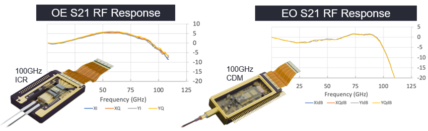
Curious about whether high bandwidth electro-optics supporting 100GHz electrical bandwidth exist?
They do and we have them.You can see the Coherent Driver Modulator (CDM) (ie. the transmitter) and Intradyne Coherent Receiver (ICR) below, along with the measured frequency response of these devices. The graphs demonstrate that 100GHz electrical bandwidth passband is achieved with the Ciena CDM and ICR designs, and that they have the requisite performance to support 200Gbaud modem operation.
An important choice: the right CMOS technology
Selecting the appropriate CMOS technology node was another important technology decision, as it dictates what functionality can be achieved at what space and power. We selected the N3E 3nm CMOS process as it provides significant performance and power benefits compared to 5nm, and the maturity of the N3E technology aligns well for 1.6 terabit product availability and network rollout in 2024.
By utilizing 3nm CMOS technology, we can achieve the programmable 1.6Tb/s line rate we need for networking while ensuring that the 1.6T modem fits within a compact footprint.
What does 3nm CMOS mean for you?
With 3nm CMOS, you can achieve 50% power per bit reduction and associated energy savings for your business. You can leverage your existing installed base, and support twice the capacity in hardware that easily slots into deployed products, without requiring any changes from a powering perspective.
 Is it possible to have 3nm coherent DSP chips in the lab today? Yes, it is. We have them.
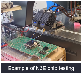
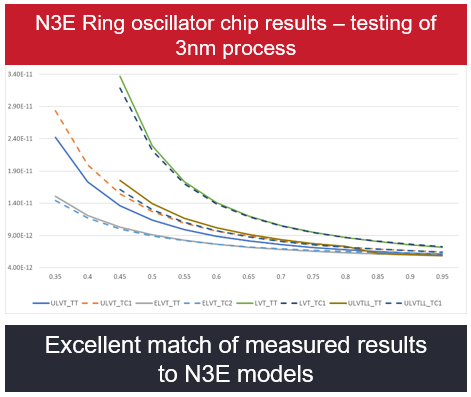
The graph below is an example of how we have verified the maturity of the N3E process through measurements, where the measured results closely match predicted models. We have also measured and verified what could arguably be the most challenging of the 200Gbaud modem design: the high bandwidth analog front end (DAC and ADC), which is another in-house design from Ciena.
Another technological hurdle squashed!
An additional advantage of using 3nm CMOS is that we have been able to integrate new DSP algorithms that increase spectral efficiency by an impressive 15% compared to WL5e, and even more in nonlinear environments. What impact will these innovations have in your network? Stay tuned for our next blog in the series to understand what to expect as part of the new DSP and the benefits of the new algorithms for your network and your business.