


Designing for programmable infrastructures – advancements in electro-optic components
Evolving coherent optical networks
Massive growth in fiber capacity demand - along with the need to have more network processing functionality at the edge - is driving network infrastructures to become more programmable and flexible. This transformation to programmable infrastructures enabling the Adaptive NetworkTM is, in turn, driving the need for continued innovation in coherent optical system design to encompass new features and capabilities and extend use cases to new areas of the network.
How is this influencing network equipment design? Addressing these features translates to different requirements for mechanical form, performance characteristics and number of modes depending on the application. These requirements are falling into two primary application sets which drive development paths today: performance-optimized solutions targeting best system performance and footprint-optimized solutions targeted to fit into a specific form factor and power envelope. System designers who also do component-level design can apply the advances in foundational technologies to meet the challenges for these new application sets.
Evolving foundational technologies
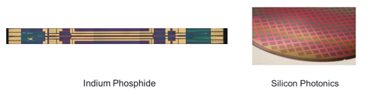
For several decades, CMOS chip designs - including DSPs for coherent modems - have benefited from greater amounts of functional integration over several generations. They have also benefited from high-yield, high volume manufacturing of multiple copies of a chip processed on - and cut from - a silicon wafer. The modem at the heart of a coherent optical system relies not just on the CMOS DSP, but also the accompanying electro-optical components to convert the electrical data signal to an optical one for fiber transmission. Emerging requirements at the network and system level are converging with new wafer scale processing for key foundational technologies for electro-optics offering the benefits of greater circuit integration, performance and manufacturability. Two process technologies underpin the electro-optical transmit and receive chains for today’s coherent systems: indium phosphide (InP) and silicon photonics (SiPhot).
Let’s take a deeper dive into electro-optics for coherent modems – and why they are critical to enabling programmable infrastructures.
Electro-optics requirements for programmable infrastructures
Fiber capacity increases over the last decade can be viewed from the perspective of Ciena’s WaveLogic DSP evolution where each successive generation has doubled the maximum capacity rate on an optical wavelength while also migrating to enhanced system capabilities with features like real-time telemetry. Through each successive generation, two key trends have gone hand in hand with innovation in coherent optical system design: the need for more tightly coupled design and packaging between the electrical and optical components and the need for greater levels of integration in both electrical and photonic circuits.
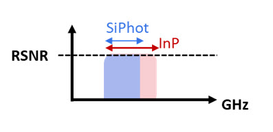
To meet new network requirements, there are challenges for the electro-optical components that must be met for each type of solution. Parameters like high-bandwidth (>50GHz) and linearity to support high-order modulation formats are required. Low power consumption is required for pluggable coherent solutions. Photonic integration is the implementation of greater levels of functionality in microscale layout and manufacturing of a single element. For both InP and SiPhot, this is a fundamental enabler for both high performance and footprint-optimized solutions.
Greater levels of functional integration in photonic circuits translate to reduced area, such as the ability to combine transmit and receive channels on the same die. Depending on the process technology used, this enables a range of performance for different coherent applications, from high-performance 800G to footprint-optimized 400ZR. It has also paved the way for joint packaging of electrical and photonic elements in different processes for higher speed and performance. Joint packaging of multiple elements also enables lower cost and simplifies assembly, leveraging the type of manufacturing flows used for semiconductor chips.
The right electro-optics technology platform for the right application
Ciena has design expertise with both InP and SiPhot which gives maximum flexibility in system design for addressing the next-generation of divergent network requirements. InP is a mature and widely deployed technology which has the advantage of being able to support high-bandwidth signals to address high-performance optical functions as well as the ability to incorporate laser sources and amplification on-chip.
SiPhot has emerged as a key technology for footprint-optimized applications owing to the high degree of photonic-electronic integration, the avoidance of hermetic packaging and the ability for system vendors to leverage high-yield fabrication processes for volume production. Choosing the appropriate material platform for the target application means factoring in the relative importance of performance, level of integration and volume scale. With new design approaches, SiPhot performance limits can be stretched and with the ability to leverage wafer scale manufacturing, InP can also be amenable to volume applications. In some cases, the optimal choice may even be a design based on a combination of both technologies.
A new wave of optimized electro-optical components
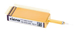
The high-bandwidth characteristics of InP have already enabled Ciena system designers to design commercially viable solutions for 400G and 800G solutions in the form of highly integrated and compact coherent driver modulator (CDM) components.
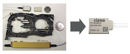
An example use case for SiPhot for a high-volume application also optimized for performance, is a micro-Integrated Coherent Receiver (or μICR). This device integrates the optical functions of a coherent receiver on a single SiPhot die and the full design is optimized through co-design and joint packaging with the trans-impedance amplifier (TIA) circuit. Owing to the ability to use non-hermetic packaging, this design is also amenable to volume manufacturing and assembly.
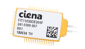
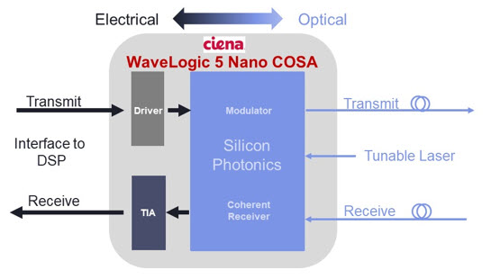
A key enabler for footprint-optimized, pluggable coherent solutions based on SiPhot is the implementation of a full coherent optical sub-assembly (COSA) into a ball-grid array (BGA) package, a favoured chip packaging option in the semiconductor domain for many years. In this case, both receive and transmit functions are integrated onto a common SiPhot die and jointly packaged with the driver and TIA elements. The ability to use non-hermetic packaging in the assembly stage reduces cost, enables volume manufacturing and allows for direct fiber attach to the package. As in the examples of μICR and CDM components, co-design of multiple elements allows for higher levels of optimization.
Pushing the envelope for electro-optical component design
As optical network system requirements diversify and design challenges intensify, this is driving further innovation in the use of photonic integrated circuits. Design improvements to increase the baud supported in SiPhot modulators and receivers will allow them to be used in high-performance systems. Ensuring that the designs are hardened – or able to support extended operating temperatures – will allow for footprint-optimized designs that can be deployed in exterior cabinets which expands the use case for coherent technology into more applications. The combined use of InP for high-efficiency, high-bandwidth modulators and SiPhot for integrated coherent receivers is another option for the next generation of coherent optical systems.
For electro-optical component design, both InP and SiPhot material platforms will have a role to play, and the ability to be able to design in both technologies will enable a forward path for programmable infrastructures.