


Building the Adaptive Network – starting with silicon
Journey to the Adaptive Network
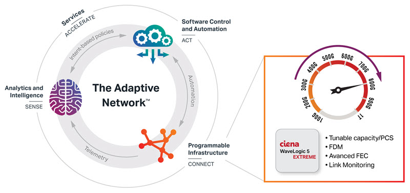
New bandwidth-intensive content and applications, along with a massive proliferation of connected devices, will place heavy demands on communications networks going forward. To prepare for this, providers must transform their networks though the implementation of new hardware and software solutions. The Adaptive NetworkTM is the ultimate goal and consists of three main elements – a programmable packet and optical infrastructure to connect network elements; an analytics and intelligence layer to analyze and predict network behavior; and software control and automation to simplify end-to-end management across multi-vendor, multi-domain networks.
A programmable infrastructure is based on network systems which can support multiple operating modes, allow for optimization of network paths through tunability, provide for scalability and support intelligence through real-time link monitoring. These capabilities contribute to a network that can adapt and scale according to demand.
Coherent DSPs: underpinning programmable infrastructures
High-speed global communications networks are based on the manipulation of photons (light), but over the last ten years semiconductor electronics has been the foundation for significant advances in the delivery of lower cost per bit and greater flexibility. Semiconductor integrated circuits (IC) have continued to increase in complexity, with each new generation of manufacturing process technology offering greater functionality, smaller area and lower power.
Fabricated primarily in silicon, IC processing technology – also referred to as CMOS – is based on large-scale integration of transistor gates as a primary building block. Each process node is notionally identified by a gate size expressed in micrometers or nanometers, although the names are typically no longer related directly. Volume manufacturing for the majority of semiconductor products is currently in “7nm” (or equivalent) from various CMOS foundries. Today’s Application Specific-ICs (ASICs) can integrate several hundred million transistors in a chip area of only few hundred mm2.
The introduction of coherent optical technology has also taken advantage of increased silicon transistor density, implementing greater amounts of complexity in signal processing to the IC driving the optical components in a coherent optical transceiver. The core of this IC is a Digital Signal Processor (DSP) which, among other functions, applies complex modulation to data signals to enable greater transmission capacity in the optical fiber. In fact, ‘DSP’ has become a de-facto term in the industry to describe semiconductor ICs for coherent optical modems.
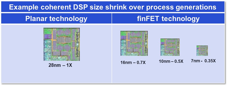
With the need for greater capacity in optical networks, as well as the need to squeeze as much performance as possible from fiber plants, DSP chips have grown significantly in transistor gate count over the last few years. To offset significant increases in power dissipation and size, coherent DSP designs have migrated to higher density, smaller gate size process nodes with each successive generation. The tenet of Moore’s Law – describing the doubling of transistor density for semiconductor process nodes every 18 month to 2 years – is somewhat analogous for coherent DSPs. With each successive DSP generation, the capacity has doubled from 100Gbps to 200Gbps to 400Gbps and, now, to 800Gbps. Using complex modulation, the baud for each generation has only had to grow by around 50%.

New economic benefits of increased capacity per wavelength were realized with each generation. Alongside this, the use of lower power, higher density CMOS nodes allowed greater levels of programmability and performance-optimizing functions.
Silicon design challenges grow
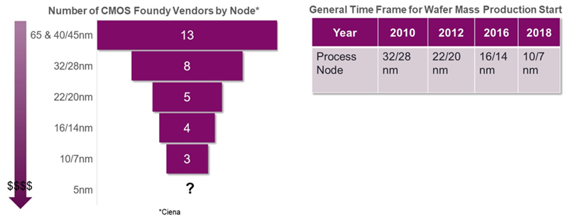
How has all of this been achieved? Not without significant investment, design skills and innovation. Looking back to 2010, roughly the time when the first 100G coherent solutions started to ramp, the semiconductor industry had already dropped from 13 to 8 vendors offering CMOS fabrication services as, in some cases, IC companies started to divest of the cost of overhead for building and running their fabs. The number of foundry vendors has reduced with each node to the point where there are currently only three primary vendors worldwide that manufacture 7nm chips. The number of vendors investing in the next 5nm node will likely not increase. Likewise, the upfront investment for companies developing coherent DSP chips is also growing.
As process nodes have transitioned to smaller geometries, we can start to understand where the challenges in coherent optical DSP designs lie. The jump from planar to finFET transistors offered more scaling for digital circuits which translated to lower power and less real estate for the same functionality.
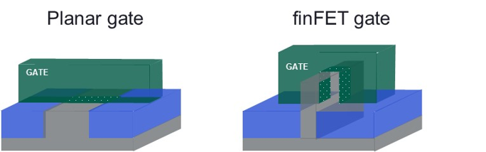
Despite the advantages offered by finFET gates for shrinkage, there are challenges in the design and implementation phases. Multiple patterning lithography for very dense interconnect means that physically laying out and connecting chip circuits is a demanding task. Although significant increases in transistor density were achieved by moving to a vertical ‘fin’ structure for the gate, this also posed greater challenges for thermal management in the design process. Indeed, for all aspects of chip design from power efficiency through to reliability, design margins are tightening with each new, smaller node.
WaveLogic 5 Extreme: Building the first 800G DSP
In realizing the WaveLogic 5 Extreme DSP, Ciena engineers have had to contend with the physical design challenges already mentioned while delivering a packaged chip size and power envelope that are suited to compact integrated and mountable form factors. Multiple configurations were implemented for tunable capacity at maximum performance, along with built-in functional capabilities to support network analytics.
Some of the advanced features implemented in the DSP include advanced Forward Error Correction (FEC), Probabilistic Constellation Shaping (PCS) and non-linear mitigation techniques, such as Frequency Division Multiplexing (FDM). A throughput-optimized FEC offers the right balance of overhead to payload ratio to maximize reach for a given capacity or, alternatively, maximize capacity for a given reach. With PCS, throughput can be selected from 200 – 800Gbps in increments of 25Gbps so operators can optimize based on system margin which, in turn, maximizes network efficiency. FDM breaks up the signal band into discrete subcarriers and renders the transmitted signal more robust to the presence of non-linearity, improving reach or capacity. Link monitoring features are also included, some based on machine learning, to enhance control and automation of networks.
Silicon for the Adaptive Network
The DSP is one of the fundamental components in coherent optical systems paving the way for network transformation. Innovation and investment in coherent DSPs ensure the continued evolution to the Adaptive Network.