


Photonic integration and co-packaging: Design tools for footprint optimization in data center networks
Advances in foundational technology underpin the DCI evolution
Data center networks have evolved rapidly over the last couple of years, in large part due to the scalability and flexibility supported by today’s compact modular DCI solutions. System designers leveraged advances in key foundational technologies to pack significant capacity and service density into these products, and their popularity is growing as these solutions capture new market segments.
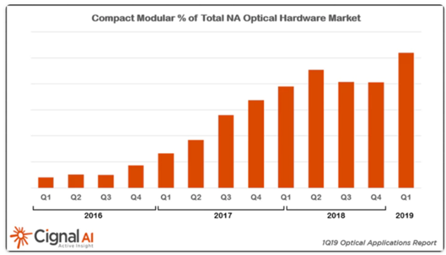
Figure 1: Forecast for compact modular coherent systems,
Source: “Compact Modular Optical Sales Expand, Reaching Over $275M”, Cignal AI, July 16, 2019
The same advances have also paved the way for new consumption models for coherent optical technology in the form of footprint-optimized, pluggable solutions . As traffic growth for server interconnect within data centers continues to increase, greater for interconnect between data centers (DCI) will be required. Scaling of data center traffic to get more bandwidth adds to the power consumption overhead and real estate requirements for operators which adds to capital and operational costs. With each new generation of switching platform and coherent optical transport systems, designers have met the challenges by increasing throughput density and reducing power/bit. Both intra-DC and DCI traffic flows will increasingly rely on advances in foundational technologies and system design options to mitigate power consumption while maximizing interconnect densities.
What are these foundational technologies? They include:
- Complementary Metal-Oxide Semiconductor (CMOS)
- Indium phosphide (InP)
- Silicon photonics (SiPhot)
In networking applications, CMOS is the basis for both high-capacity switch chips used in router platforms and coherent optical digital-signal-processors (DSP). InP and SiPhot are used to build electo-optical circuits for signal transport over optical fibers. Together, the DSP and electro-optical components are the heart of coherent optical transport systems.
More tools in the design toolbox
Communications networks have benefited from advances in semiconductor technology, particularly the effects of Moore’s Law, where CMOS integrated circuits have doubled in transistor density every couple of years. For optical networks, the application of coherent optical signaling ushered in the era of extremely high fiber optic line rates per wavelength over terrestrial and submarine links alike. With each successive CMOS generation, greater silicon transistor densities have allowed for significant increases in DSP operations/second to be supported by chips of the same size and power such that system-level space and thermal constraints were not exceeded. Coherent optical DSP designers take advantage of higher transistor densities per CMOS node in two ways:
- Greater amounts of signal processing enabled the design of high-performance solutions with greater capacity and greater functionality
- More compact, low-power designs to support footprint-optimized or dedicated applications
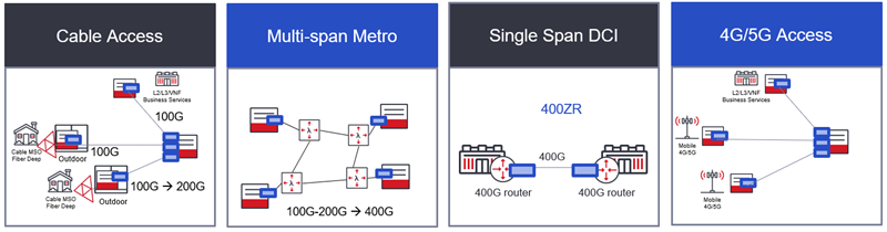
Figure 2: Applications for Coherent Pluggable Solutions
High-performance switch chips for router platforms have also capitalized on Moore’s Law and switching capacity has doubled ever couple of years. In parallel, the electro-optic components based on InP and SiPhot that interface to DSPs in coherent optical systems have evolved in power and area to enable both higher performance and new, compact designs. Greater levels of functional integration in foundational processes, along with a wider array of manufacturing and assembly options at the component package level, are adding to the tools in system designers’ toolboxes.
What are photonic integration and co-packaging?
The terms ‘photonic integration’ and ‘co-packaging’ are being used with increasing regularity in discussions about the future of data center switch fabric and optical transport. They are sometimes used interchangeably to describe the general trend of reduction in size and power while increasing functionality and/or performance capability of a solution. Both design methodologies are key tools to enable the next generation of footprint-optimized systems for data center networks.
Integration is typically the implementation of a greater number of circuits (optical or electrical) and functional blocks within a common manufacturing chemistry, or process technology flow (such as CMOS or InP).
Co-packaging, by contrast, is the implementation of different constituent elements from different manufacturing processes within a common enclosure or mounted on a common substrate. Effectively, this is package-level integration.
In both cases miniaturization is the goal, and this driven by the need for the system to support either:
- Greater functionality within the same space and power envelope or
- Smaller area and lower power for the same functionality in a new generation product
CMOS technology is a long-standing example of integration. Increased transistor density with each new process node allows for more functional blocks to be embedded into a single design where some of these functions were previously in discrete devices mounted on a system circuit board. Likewise, the migration from lithium niobate (LiNbO 3 ) to InP and SiPhot, as the manufacturing base for the electo-optics chain in a coherent optical system, has been a key enabler to achieve required performance and functionality in smaller footprints via the implementation of photonic integrated circuits.
Welcome back, MCM
Co-packaging of different chip elements, or die, is not a new concept or approach. Processors for high-performance super-computing have taken this approach in the past, often referred to as a Multi-Chip Module (MCM). Moving forward, more advanced packaging options - such as fan-out, 2.5D and 3D which have significantly greater amounts of intra-chip interconnect - will provide system designers with options for building in more functionality while streamlining designs and optimizing interfaces.
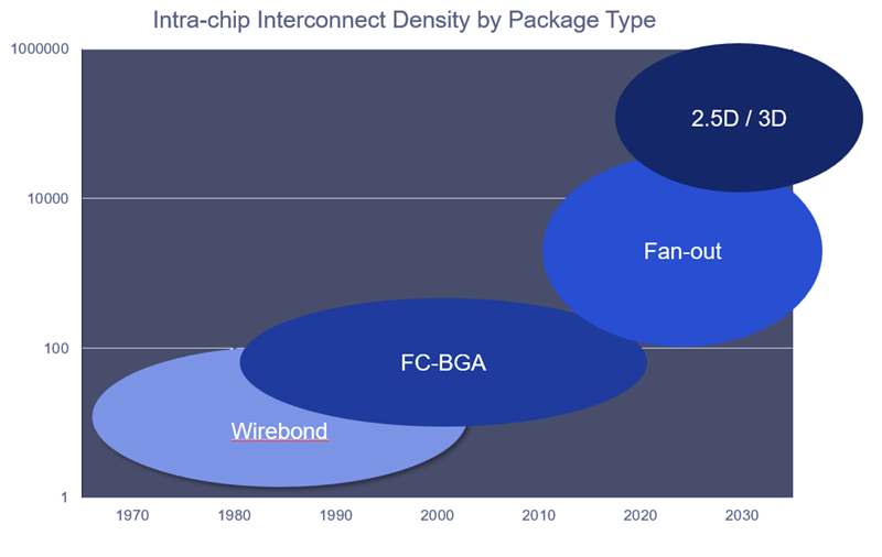
Figure 3: Order of magnitude increase in interconnect density by package type
There has been a resurgence of interest in taking the MCM approach to system design at the chip and component level in various industries, and this is being driven by a variety of factors including:
- The significant increase in cost for designing in new CMOS nodes
- Varying performance requirements for the different sub-blocks of a CMOS chip design
- The need to combine multiple die, based on different process technologies, in a compact form or on a common substrate
At 7nm, the most advanced CMOS node currently in mass production, the cost of chip development and manufacturing is very high. For applications where scaling of area and reduction of the total power dissipation of the chip are critical, having the entire chip design in the same node on one, monolithic die makes sense only if the various elements (digital logic, analog and memory blocks) can all take advantage of power and area scaling while also maintaining performance characteristics.
Significantly higher performance requirements for analog blocks in new applications may dictate the need for using base technologies – such as Bipolar CMOS (BiCMOS) - that can support these requirements and this, in turn, may lead to co-packaging of separate die for analog and digital functionality.
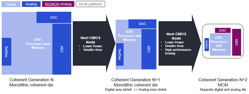
Figure 4: Potential path forward for coherent optical MCM
Finally, some applications require a mix of not only advanced analog and digital functionality but also the use of dedicated process technologies such as InP and SiPhot which are the basis for today’s electro-optical transmission circuits.
Using the design tools for power optimization: switch chip evolution
In hyperscale data center switch fabrics, the capacity of switch chips has enabled massive scaling from one generation to the next. The latest generation supports over 12Tbps of switching capacity from a single device which is equivalent to 32 x 400G Ethernet ports. Subsequent switch chips are projected to double the capacity to over 25Tbps and again to 50Tbps. Increases in CMOS transistor density are just about able to support this scaling to prevent the physical size of the chips from growing too large. Where the limits are really occurring is at the chip edge; getting the signals off the package and across the system board to the next device.
Up to and including the current switch chip generation, the electrical signal input/output (I/O), otherwise known as serializer/deserializer (SerDes) interfaces support up to just over 50Gbps capacity with some overhead for error correction – up to 56Gbps. At this generation of chip-to-chip signaling, the use of higher-order modulation has been necessary to increase the signaling capacity which keeps the actual signal rate lower. Pulse-Amplitude-Modulation with four levels (PAM-4) is employed which encodes 2 bits/symbol transmitted. The symbol rate for 56Gbps SerDes is then only 28GBaud (symbols/sec).
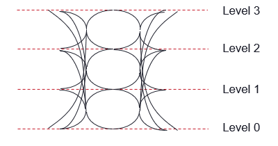
Figure 5: PAM-4: Four combinations of 2 logic bits encoded as 2 bits/symbol
As the industry moves to the 50Tbps generation of switch chips, the I/O density will have to keep up. A straightforward solution is to increase the SerDes bit rate or complexity of modulation (more bits/symbol), but that puts a strain on signal integrity and adds challenges for system board design. As the goal is to maintain power and area constraints, this is not an inexhaustible route forward.
General expectations are that the industry will look to the advantages of photonic integration and co-packaging and that the switch chip I/O will move from electrical to optical. Two of the big hyperscale data center operators, Microsoft and Facebook, recently announced the Co-Packaged Optics (CPO) collaboration, an initiative to investigate options for co-packaging of optics with switch chips.
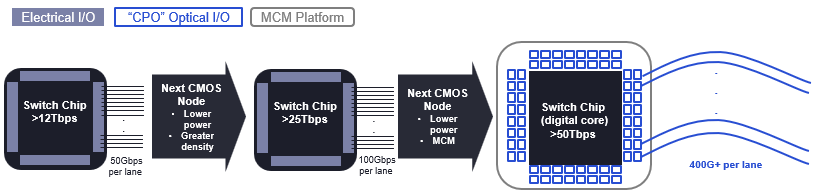
Figure 6: Potential path forward for switch chip MCM
Using the design tools for footprint optimization: coherent optical
Coherent optical transmission system design has already migrated into new applications areas to target specific segments of the network where minimizing power and area are key requirements. An example of a footprint-optimized application, supporting high-capacity transmission and constraining the reach to 80 – 100km, is the OIF’s 400ZR initiative for DCI. Leveraging advancements both in photonic integration and the ability to pack significant amounts of processing in coherent DSPs, 400ZR will fit in compact, pluggable forms like QSFP-DD and OSFP. The implementation of coherent technology in compact form factors has meant trade-offs in performance are required.
For future generations of single-span DCI coherent solutions that interface with high-radix switch chips, design trade-offs will need to be made again. Migrating coherent solutions from faceplate, pluggable optical modules to co-packaged, board-mounted optical transceivers capable of driving DWDM signals over tens of km will not be straightforward. Nor is this evolutionary pathway necessarily the best or only route forward. Considerations on whether co-packaging of photonics with coherent DSPs is warranted will likely include:
- The need for optical I/O compatibility on the client side of the coherent modem with next-generation switch chips
- The requirements for photonics used for line-side transport
In the first case the migration from electrical switch I/O to optical will drive the need for a compatible short-reach (chip-to-chip or chip-to-module) optical I/O on the client-side of a coherent modem. On the line-side, the options for photonics will be governed by requirements for performance, power, thermal management, and volume manufacturability (yield and cost).
Fully incorporating the line-side photonic integrated circuits and other electro-optical components into MCMs using interposers are one step. A step further still, will be CMOS and photonics processed on the same wafer. The co-packaging of optics and CMOS for coherent solutions to that degree will only happen when either performance trade-offs can be made, or the co-packaged foundational technology performance catches up to the level needed.
Ciena’s coherent toolbox
As market-leading participant in the evolution of DCI networks , and an industry leader in coherent optical technology, Ciena has been able to leverage ownership of foundational technologies to maintain the pace of innovation needed for each new generation of network applications. And as network requirements have diverged for different applications, the ability to optimize through co-design of the different foundational elements has played a key role in Ciena’s ability to deliver differentiated solutions to the market including pluggable coherent products.
As new component-level architectures emerge, only those companies with the full suite of capabilities in foundational technologies, a deep knowledge of networking requirements and experience in delivering a range of system solutions will be in a position to address evolving network architectures.