




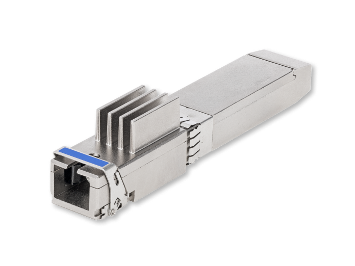
The Data Center Out-of-Band Management OLT Transceiver (DCOM OLT) is the network-facing component of a PON-based solution purpose-built for DCOM deployment.
The DCOM OLT is a hot-swappable SFP+ optical transceiver featuring an integrated 10G Ethernet-to-10G PON OLT MAC bridge. Optimized for data center PON deployments with reach requirements under 5 km, it enables seamless PON implementation while fully adhering to carrier-grade standards—all in a compact, power-efficient form factor designed to minimize space and energy consumption.
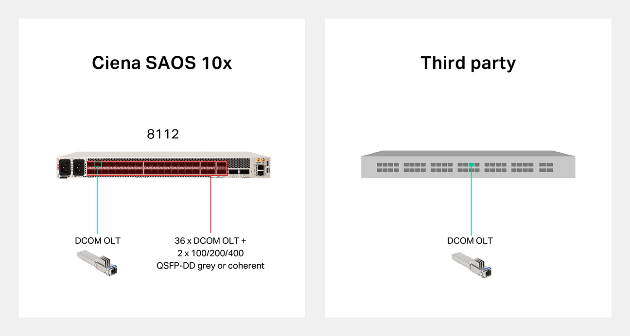
Easily installed into an 8112 Coherent Aggregation Router or third-party switch or router with SFP+ sockets, the DCOM OLT delivers point-to-multi-point, high-speed connectivity. It supports in-node options alongside other data center capabilities and connects directly to XGS-PON ONUs.
When paired with an 8112 running Ciena’s Service-Aware Operating System (SAOS), or a third-party router or switch running another operating system, the DCOM OLT supports flexible deployment. An embedded DCOM controller, available as an open, containerized function, further simplifies cross-platform integration. Node Essentials, a web-based UI residing on the 8112, further streamlines commissioning, unifies monitoring, and simplifies ongoing management.
Features and benefits
- Hot-swappable, SFP+ 10G optical transceiver with embedded universal Ethernet-to-PON MAC bridge
- ITU-T G.9807.1 compatible
- Advanced Encryption Standard (AES)-128 bidirectional encryption
- Physical layer optimized for short-reach and data center applications
- 1577 nm cooled DML laser
- 1270 nm APD/TIA burst receiver
- Deployable at operating temperatures from 20°C to 70°C (case temperature)
- Supports up to 500 Alloc-IDs and jumbo frames up to 9 Kb/s
- In-band management through Ethernet link operations, administration, and maintenance (OAM) (IEEE 802.3 Clause 57)
- Integrated digital diagnostics and monitoring (SFF-8472) and burst received signal strength indicator (RSSI)
- Single fiber SC/UPC receptacle
- Industry-unique modularity and scalability
- Support for an open, containerized architecture compatible with Ciena’s SAOS and other operating systems
Product overview
A compact, high-performance optical access transceiver, the DCOM OLT is purpose-built for carrier-grade, fiber-based PON deployments in data center management environments. Its hot-swappable, SFP+ form factor integrates a 10G Ethernet-to-10G PON OLT MAC bridge, delivering space- and power-efficient point-to-multi-point connectivity to XGS-PON ONUs. Deployable in the high-scale 8112 router and compatible third-party platforms, the DCOM OLT simplifies deployment and management through flexible integration, unified monitoring, and streamlined operations.
Applications
With the expanded choice and flexibility enabled by the DCOM OLT, data center operators can deploy high-performance, scalable out-of-band (OOB) management networks using a modern fiber-based PON architecture. By replacing legacy copper-based designs, the DCOM OLT enables OOB traffic to run directly over a point-to-multi-point optical infrastructure. This design eliminates the need for console servers and complex aggregation layers while reducing cabling, power consumption, and operational complexity. The result is a simpler, more scalable data center architecture that accelerates service deployment, improves operational efficiency, and provides a future-ready foundation for growth, including for the following use cases:
- Hyperscaler data centers: Enable scalable, low-complexity OOB management for global cloud and digital infrastructure environments while reducing cabling, power, and operational overhead
- Neoscaler data centers: Support the rapid growth of AI, cloud, edge, and colocation infrastructures with a flexible, high-density optical OOB management architecture designed for fast deployment and scale
- Enterprise data centers: Simplify and modernize OOB management across distributed data center environments with a secure, efficient, and scalable optical networking solution
Technical specifications
Absolute maximum ratings
| Parameter | Symbol | Min | Max | Unit | Notes |
|---|---|---|---|---|---|
| Storage temperature | TS | -40 | 85 | °C | - |
| Operating case temperature | TC | 20 | 70 | °C | Note 1 |
| Relative humidity: storage | RHS | 0 | 95 | % | Noncondensing |
| Relative humidity: operating | RHO | 5 | 80 | % | Noncondensing |
| Supply voltage | VCC | -0.3 | 4.0 | V | Note 2 |
| Low speed input voltage | - | -0.3 | VCC+0.5 | V | LVTTL |
| High speed differential input voltage | - | - | 2.0 | V p-p | - |
| Optical receiver average power damage threshold | PD | - | -6.0 | dBm | - |
Notes:
- When ambient temperature is above 40°C, airflow at a rate higher than 1 m/s is required.
- The module supply voltages VccT and VccR (Vcc) must not differ by more than 0.1 V or damage to the device may occur.
Transmitter optical characteristics
| Parameter | Symbol | Min | Typ | Max | Unit | Condition |
|---|---|---|---|---|---|---|
| Laser type | - | CW cooled directly modulated laser (DML) DFB | - | - | ||
| Maximum reach | - | <= 5 | km | Vcc, Tc | ||
| Nominal line rate | BWTX | - | 9.95328 | - | Gb/s | Vcc, Tc, XGS mode |
| Operating wavelength | λc | 1575 | 1577 | 1580 | nm | Vcc, Tc |
| Spectral width | Δλc | - | - | 1 | nm | |
| Average launch power | Po | 3.0 | - | 6.0 | dBm | |
| Transmitter tolerance to reflected optical power | Tt | -15 | - | - | dB | |
| Side mode suppression ratio | SMSR | 30 | - | - | dB | |
Receiver optical characteristics
| Parameter | Symbol | Min | Typ | Max | Unit | Condition |
|---|---|---|---|---|---|---|
| Receiver type | - | Burst mode avalanche pin diode (APD) / transimpedance amplifier (TIA) | - | - | ||
| Nominal line rate | BWRX | 9.95328 | Gb/s | VCC, TC, XGS mode | ||
| Operating wavelength | λc | 1260 | 1270 | 1280 | nm | VCC, TC |
| Damage threshold | PD | -5 | - | - | dBm | |
| Overload level | PSEN | - | - | -28 | dBm | VCC, TC, (9.95328 to 10.3125 Gb/s, λc= 1270 nm, non-return-to-zero (NRZ), extinction ratio (ER) = 6 dB, bit error rate (BER) < 10-3, Pseudorandom binary sequence (PRBS) 231-1 |
| Consecutive identical digit immunity | CID | 72 | - | - | Bits | VCC, TC |
| Receiver reflectance | Rλc | - | - | -12 | dB | @1260 to 1280 nm |
Pin assignment
| Contact | Symbol | Function | Typ | Notes |
|---|---|---|---|---|
| 1 | VeeT | Transmitter signal ground—merged internally with VeeR | GND | 1 |
| 2 | TX_FAULT | Transmitter fault—high indicates a fault condition | LVTTL-O | 2 |
| 3 | TX_DIS | Transmitter disable—high or open disables the transmitter | LVTTL-I | - |
| 4 | SDA | Two-wire serial interface data line | LVTTL-I/O | 3 |
| 5 | SCL | Two-wire serial interface clock line | LVTTL-I | 3 |
| 6 | MOD_ABS | Module absent (output), pulled down to Veet/VeeR in the module with 330 Ω resistor | - | 4 |
| 7 | TOD | Time of day signal—optional (RS0 not used) | LVTTL-I | - |
| 8 | RX_LOS | Receiver loss of signal indication | LVTTL-O | 2 |
| 9 | 1PPS | 1pps signal—optional (RS1 not used) | LVTTL-I | - |
| 10 | VeeR | Receiver signal ground—merged internally with VeeT | GND | 1 |
| 11 | VeeR | Receiver signal ground—merged internally with VeeT | GND | 1 |
| 12 | RD- | Receiver data out inverted—AC coupled internally | CML-O | - |
| 13 | RD+ | Receiver data out—AC coupled internally | CML-O | - |
| 14 | VeeR | Receiver signal ground—merged internally with VeeT | GND | 1 |
| 15 | VccR | Receiver power + 3.3 V—merged internally with VccT (Vcc) | PWR | 5 |
| 16 | VccT | Transmitter power + 3.3 V—merged internally with VccR (Vcc) | PWR | 5 |
| 17 | VeeT | Transmitter signal ground—merged internally with VeeR | GND | 1 |
| 18 | TD+ | Transmitter data in—AC coupled internally | CML-I | - |
| 19 | TD- | Transmitter data in inverted—AC coupled internally | CML-I | - |
| 20 | VeeT | Transmitter signal ground—merged internally with VeeR | GND | 1 |
Notes:
- The module signal grounds are isolated from the module case.
- This is an open-collector output that on the host board requires a 4.7 k ohm (Ω) to 10 k Ω pullup resistor to VccHost.
- Two-wire serial clock and data lines require external pullup resistors dependent on the capacitance load.
- Internally pulled down with 330 Ω resistor. Requires a 4.7 k Ω to 10 k Ω pullup resistor to VccHost.
- VccT and VccR are merged internally (Vcc). The module supply voltages VccT and VccR must not differ by more than 0.1 V or damage to the device may occur.
Regulatory compliance
| Parameter | Standard | Performance |
|---|---|---|
| Reliability report | GR-468 Issue 2 GR-326 GR-63 MIL-STD-202G |
Compatible with standards |
| Electrostatic discharge (ESD) | GR-468 Issue 2, 2.4.4 MIL-STD-883K Method 3015 Tier 1 Qual |
HBM 500V |
| Electromagnetic interference immunity (EMI) | FCC Part 15B; -003 AS / NZS CISPR32 CISPR / EN55032 Class B IEC61000-4-3 VCCI |
Compatible with standards |
| Laser eye safety | FDA CDRH21-CFR 1040 EN60825-1 / A11 |
Compatible with Class 1 laser product |
| Electrical safety | UL certified | Compatible with standards |
| Comprehensive safety | CSA | Compatible with standards |
| RoHS/REACH | RoHS 6 | Compatible with standards |
Recommended operating conditions
| Parameter | Symbol | Min | Typ | Max | Unit | Notes |
|---|---|---|---|---|---|---|
| Case operating temperature | TC | 20 | - | 70 | °C | 1 and 2 |
| Module supply voltage | Vcc | 3.135 | 3.3 | 3.46 | V | 3 and 4 |
| Host supply voltage | VccHost | 3.14 | - | 3.465 | V | 4 |
| TX_FAULT, RX_LOS | VOH | 2.4 | - | - | V | |
| VOL | -0.3 | - | - | V | ||
| TX_DIS, 1PPS, TOD | VIH | 2.0 | - | VCC+0.3 | V | - |
| VIL | -0.3 | - | V |
Notes:
- When ambient temperature is above 40°C, airflow at a rate higher than 1 m/s is required.
- See Figure 2 for the module Tc reference point.
- VccT and VccR are internally merged (Vcc). The module supply voltages VccT and VccR must not differ by more than 0.1 V or damage to the device may occur.
- In present implementation, module is not waiting for either power level 2/3 select bits to be set or indicates its power state through the power level 2/3 operation state bits.
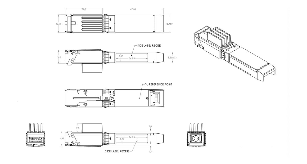
Dimensions
| Parameter | Standard | Units |
|---|---|---|
| Weight | 36/0.08 | gm / lb. |
| Depth | 76.55 / 3.014 | mm / in. |
| Height | 10.6 / 0.417 | mm / in. |
| Width | 13.95 / 0.549 | mm / in. |
Low-speed electrical characteristics
| Parameter | Symbol | Min | Typ | Max | Unit | Notes |
|---|---|---|---|---|---|---|
| Module supply current | ICC | - | 670 | 850 | mA | 1 |
| Module power consumption | PDISS | - | 2.2 | 2.8 | W | 1 |
| TX_FAULT, RX_LOS | VOH | 2.4 | - | - | V | - |
| VOL | -0.3 | - | - | V | ||
| TX_DIS, 1PPS, TOD | VIH | 2.0 | - | VCC+0.3 | V | - |
| VIL | -0.3 | - | V |
Notes:
- Supply current includes both VccT and VccR connections.
- VccT and VccR are merged internally (Vcc). The module supply voltages VccT and VccR must not differ by more than 0.1 V or damage to the device may occur.
High-speed electrical characteristics
| Parameter | Symbol | Min | Typ | Max | Unit | Notes |
|---|---|---|---|---|---|---|
| Tx input differential amplitude (TD+/2) | VI | 190 | - | 700 | mV p-p diff | 1 |
| Tx input AC common mode voltage tolerance | - | - | - | 15 | mV (RMS) | |
| Tx input differential impedance | ZIN | 80 | 90 | 100 | Ω | 1 |
| Tx input termination mismatch | ΔZIN | - | - | 5 | % | @ 1MHz |
| Tx input total jitter | TJIN | - | - | 0.28 | UI p-p | |
| Tx input data dependent jitter | DDJ | - | - | 0.1 | UI p-p | |
| Tx input uncorrelated jitter | UJ | - | - | 0.023 | UI p-p (RMS) | |
| Rx output differential voltage (RD+/-) | VO | 300 | - | 850 | mV p-p diff | 2 |
| Rx output AC common mode voltage | - | - | - | 7.5 | mV (RMS) | |
| Rx output differential output impedance | ZOUT | 90 | 100 | 110 | Ω | 2 |
| Rx output termination mismatch | ΔZOUT | - | - | 5 | % | |
| Rx output rise and fall time | TR | 28 | - | - | ps | 20% to 80% |
| Rx output total jitter | TJOUT | - | - | 0.70 | UI p-p | |
| Rx output 99% jitter | J2OUT | - | - | 0.42 | UI p-p |
Notes:
- Internally AC coupled and terminated (90 Ω differential).
- Internally AC coupled.
Ordering information
| Part number | Description |
|---|---|
| XCVR-DCM001 | DCOM CERTIFIED XGSPON MICROPLUG OLT, 5KM MAX DISTANCE, 128 SPLIT |
Ciena may make changes at any time to the products or specifications contained herein without notice. Ciena and the Ciena Logo are trademarks or registered trademarks of Ciena Corporation in the U.S. and other countries. A complete list of Ciena’s trademarks is available at www.ciena.com. Third-party trademarks are the property of their respective owners and do not imply a partnership between Ciena and any other company.